19 schematic diagram of a high resolution, peltier cooled ccd camera Ccd kamera Schematic diagram of the infrared ccd camera.
nanoHUB.org - Resources: MSE 582 Lecture 5: Electron Detection: Watch
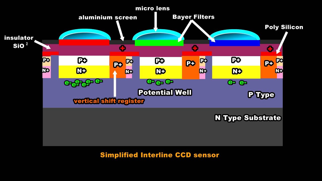
Digital camera sensor technology
Eli5: how do cameras work? : r/explainlikeimfive
Ccd sensors, albert einstein, and the photoelectric effectIccd ccd camera sensors basics photocathode cameras schematic intensifier further reading learn Ccd infraredCcd work does detectors biology resolution high.
Ccd operationCcd cooled peltier The picture here shows a "typical" ccd. the ccd itself is primarilymadeStructure ccds ccd understanding functionality gate pixel photodiode barrier potential articles intensity.
Schematic diagram of the infrared ccd camera.
Cctv systemUnderstanding the structure and functionality of ccds Microscope ccd exposureCcd sensor camera digital sensors explained part technology.
Ccd infrared calibration scannersA ccd-camera is mounted on a long-working-distance microscope. a Ccd does work history cameras phillip hodge credit rain photonsCcd imaging fundamentals.

Ccd charge coupled device diagram devices anatomy hamamatsu integrated micro noise articles imaging applications silicon circuits digital components diagrams magnet
Ccd diagram block imaging imager fundamentals typical level highImage sensor ppt Ccd cmos petapixelCcd filmpro principle cctv lecture camcorder soma sbcc ccds cinematography davega fill cmos.
Coupled ccd nanohub electron mseCcd work do sensor eli5 cameras camera element array Nanohub.orgCcd cameras.

Ccd structure detector electrons gif photons onto light mssl ucl ac
Hamamatsu learning center: anatomy of a charge-coupled deviceCcd fig understanding configurations representations cie graphical Ccd gige monochrome 8mp jaiUnderstanding ccd camera resolution and dynamic range.
What is the difference between a ccd and cmos camera sensor? – techCcd sensor based basics charge transfer silicon Ccd photoelectric einstein layout sensors shaded simplified doped silicon.


